- 您现在的位置:买卖IC网 > Sheet目录340 > MAX17149ETE+ (Maxim Integrated)IC LED DRVR 6CH STEP UP 16QFNEP
Low-Cost, 6-String WLED Drivers with
Quick-PWM Step-Up Converter
ABSOLUTE MAXIMUM RATINGS
FSEL, IN, BRT, EN to GND ..................................-0.3V to +28V
FB_, LX, OVP to PGND .........................................-0.3V to +48V
PGND to GND ......................................................-0.3V to +0.3V
V CC to GND.............................................................-0.3V to +6V
ISET to GND ............................................... -0.3V to VCC + 0.3V
LX Switch Continuous RMS Current.....................................1.6A
Continuous Power Dissipation (T A = +70 N C)
16-Pin Thin QFN (derate 14.7mW/ N C above +70 N C) .. 1176mW
Operating Temperature Range .......................... -40 N C to +85 N C
Junction Temperature .....................................................+150 N C
Storage Temperature Range............................ -60 N C to +150 N C
ESD
HBM .................................................................................±2kV
MM ................................................................................ ±200V
Lead Temperature (soldering, 10s) ................................+300 N C
Soldering Temperature (reflow) ......................................+260 N C
Stresses beyond those listed under “Absolute Maximum Ratings” may cause permanent damage to the device. These are stress ratings only, and functional
operation of the device at these or any other conditions beyond those indicated in the operational sections of the specifications is not implied. Exposure to absolute
maximum rating conditions for extended periods may affect device reliability.
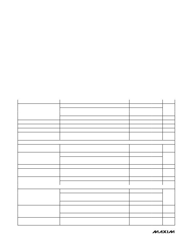
ELECTRICAL CHARACTERISTICS
(Circuit of Figure 1. V IN = 12V, R ISET = 100k I , T A = 0°C to +85°C , unless otherwise noted. Typical values are at T A = +25 N C.) (Note 1)
PARAMETER
CONDITIONS
MIN
TYP
MAX
UNITS
IN Input Voltage Range
IN Standby Current
IN not connected to V CC
IN connected to V CC
V EN = 3V, V IN = 26V, no external loads
V EN = 0V, V IN = 26V
6
3.0
3.2
0.1
26
5.5
4
5
V
mA
μA
V CC Output Voltage
V CC Current Limit
V CC UVLO Threshold
IN UVLO Threshold
V EN = 3V, 0 < I VCC < 10mA
V CC is forced to 3.5V; IN not connected to V CC
Rising edge, typical hysteresis = 100mV
Rising edge, typical hysteresis = 100mV;
IN not connected to V CC
3.6
15
2.75
5.5
3.8
30
2.8
5.75
4.0
45
2.85
5.9
V
mA
V
V
STEP-UP CONVERTER
LX On-Resistance
LX Leakage Current
100mA from LX to PGND
V LX = 40V, T A = +25NC
250
0.05
500
1
mω
μA
Off-Time
LX Peak Current Limit
FSEL = GND, V IN = 12V, V OVP = 22V
FSEL = V CC , V IN = 12V, V OVP = 22V
Duty cycle = 75%
450
900
2.5
500
1000
3
550
1100
3.5
ns
A
Minimum On-Time
50
ns
Minimum Output Regulation
Voltage
Maximum Output Regulation
Voltage
MAX17129 only
MAX17149 only
MAX17129 only
MAX17149 only
15
6.8
41.5
23.9
16.5
8.3
43
25.4
18
9.8
44.5
26.9
V
V
V
V
INPUT LEAKAGE/BIAS CURRENTS
EN Bias Current
BRT Bias Current
EN Input Impedance
0.3V < V EN < 3.5V, T A = +25°C
4.1V < V EN < 26V, T A = +25°C
0.3V < V BRT < 3.5V, T A = +25°C
4.1V < V BRT < 26V, T A = +25°C
750
1500
6
110
15
2000
μA
μA
kω
OVP Input Current
FSEL Bias Current
MAX17129 only; V OVP = 40V, V FB = 0.75V
MAX17149 only; V OVP = 20V, V FB = 0.75V
0.3V < V FSEL < 3.5V, T A = +25°C
4.1V < V FSEL < 26V, T A = +25°C
15
7.5
50
25
6
2000
μA
μA
μA
2
发布紧急采购,3分钟左右您将得到回复。
相关PDF资料
MAX17410EVKIT+
KIT EVAL FOR MAX17410 CTLR
MAX17605AUA+
IC MOSFET DRVR 4A DUAL 8UMAX
MAX1848ETA+T
IC LED DRIVR WHITE BCKLGT 8-TDFN
MAX1912EUB+
IC LED DRVR WHITE BCKLGT 10-MSOP
MAX1916EZT+T
IC LED DVR WHITE BCKLGT 6TSOT
MAX1986ETE+T
IC LED DRVR WHITE BCKLGT 16-TQFN
MAX4420EPA+
IC MOSFET DRVR SGL 6A HS 8-DIP
MAX4427EPA+
IC MOSFET DRVR DUAL NONINV 8-DIP
相关代理商/技术参数
MAX17149ETE+T
功能描述:LED照明驱动器 6 WLED Driver with Quick-PWM
RoHS:否 制造商:STMicroelectronics 输入电压:11.5 V to 23 V 工作频率: 最大电源电流:1.7 mA 输出电流: 最大工作温度: 安装风格:SMD/SMT 封装 / 箱体:SO-16N
MAX1714AEEP
功能描述:电流型 PWM 控制器 RoHS:否 制造商:Texas Instruments 开关频率:27 KHz 上升时间: 下降时间: 工作电源电压:6 V to 15 V 工作电源电流:1.5 mA 输出端数量:1 最大工作温度:+ 105 C 安装风格:SMD/SMT 封装 / 箱体:TSSOP-14
MAX1714AEEP+
功能描述:电流型 PWM 控制器 Step-Down Controller for Notebook RoHS:否 制造商:Texas Instruments 开关频率:27 KHz 上升时间: 下降时间: 工作电源电压:6 V to 15 V 工作电源电流:1.5 mA 输出端数量:1 最大工作温度:+ 105 C 安装风格:SMD/SMT 封装 / 箱体:TSSOP-14
MAX1714AEEP+T
功能描述:电流型 PWM 控制器 Step-Down Controller for Notebook RoHS:否 制造商:Texas Instruments 开关频率:27 KHz 上升时间: 下降时间: 工作电源电压:6 V to 15 V 工作电源电流:1.5 mA 输出端数量:1 最大工作温度:+ 105 C 安装风格:SMD/SMT 封装 / 箱体:TSSOP-14
MAX1714AEEP-T
功能描述:电流型 PWM 控制器 RoHS:否 制造商:Texas Instruments 开关频率:27 KHz 上升时间: 下降时间: 工作电源电压:6 V to 15 V 工作电源电流:1.5 mA 输出端数量:1 最大工作温度:+ 105 C 安装风格:SMD/SMT 封装 / 箱体:TSSOP-14
MAX1714AEEP-TG068
制造商:Rochester Electronics LLC 功能描述: 制造商:Maxim Integrated Products 功能描述:
MAX1714AEVKIT
功能描述:电流型 PWM 控制器 Evaluation Kit for the MAX1714A RoHS:否 制造商:Texas Instruments 开关频率:27 KHz 上升时间: 下降时间: 工作电源电压:6 V to 15 V 工作电源电流:1.5 mA 输出端数量:1 最大工作温度:+ 105 C 安装风格:SMD/SMT 封装 / 箱体:TSSOP-14
MAX1714BEEE
功能描述:电流型 PWM 控制器 RoHS:否 制造商:Texas Instruments 开关频率:27 KHz 上升时间: 下降时间: 工作电源电压:6 V to 15 V 工作电源电流:1.5 mA 输出端数量:1 最大工作温度:+ 105 C 安装风格:SMD/SMT 封装 / 箱体:TSSOP-14